In-body sensors, also known as implantable sensors or bio-implants, are devices designed to be inserted into the human body to monitor various physiological parameters or deliver therapeutic treatments. These sensors can provide real-time data about the body’s internal conditions, allowing for continuous monitoring and analysis. They are typically used in medical applications and can be used for diagnostics, disease management, or research purposes. In-body sensors offer unique advantages in the context of chronic disease management, including:
– Spatial resolution: access to local environment, direct and sensitive measure of specific parameters
– Temporal resolution: sense onset of events and conditions, enabling timely interventions
– Closed-loop : adaptive, personalized, targeted and automated therapy
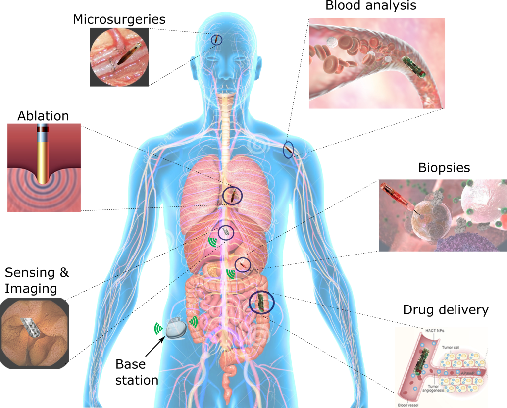
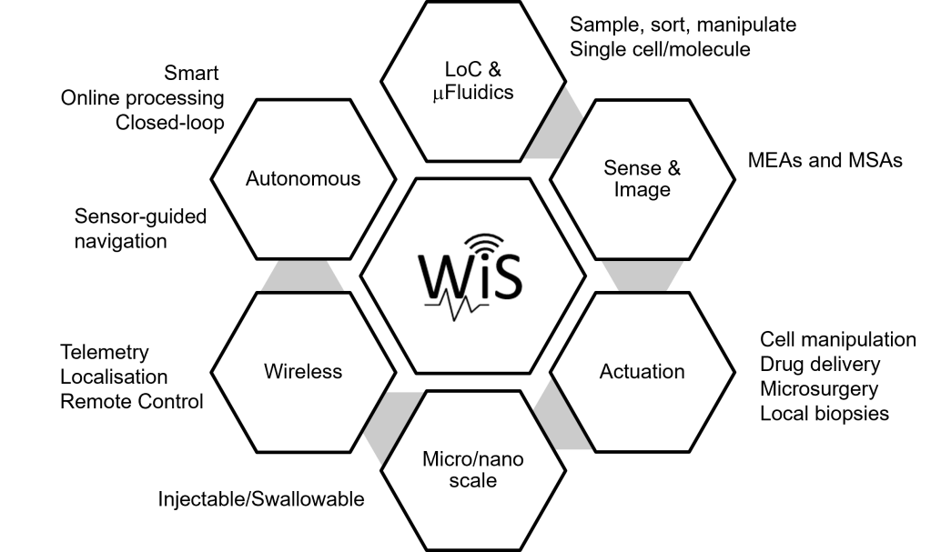
Our research focuses on the integration of CMOS, MEMS technologies to develop multi-analyte, multimodality and long-term sensing and actuating miniaturized platforms for lab-on-a-chip, injectable and swallowable sensing and actuating devices. We take a holistic approach and consider the interaction of all the primary components of a wireless sensor system, including the biointerface, the readout electronics and the wireless units. We study novel ways to integrate and miniaturize these components with focus on power efficiency and cost-effective microfabrication processes.
Focus
Ultra-Low-Power (ULP) Wireless Sensor Readouts
Wireless sensors are poised to play a pivotal role in future disease management. By developing mm-scale smart insertable/injectible medical sensors, we can enable minimally invasive remote monitoring of patient’s chronic conditions and, in turn, drive more efficient therapies. The need for sensor miniaturization however precludes the use of batteries, resorting to alternative forms of energy, either harvested from the local environment or external sources. In either case the power available at the sensor node is in the mW range and below. To retain useful sensor functionality, innovative solutions are needed to push the boundaries of power consumption and energy-efficiency of the sensor readout units. The WiS Lab addresses these challenges by developing sensor interfaces based on the integration of a number of ULP design strategies, including:
o Analog-to-time conversion (ATC) and time-based signal processing.
o Dynamic amplifiers and comparators
o Multi-sensor reconfigurable front-ends
o Pulse modulation (PM) wireless schemes for power efficient high-speed data transfer
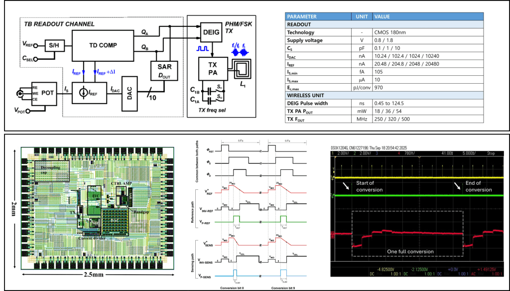
PROJECT: Time-based current-input SAR ADC potentiostat for amperometric biosensors
Designer: H. Ashrafirad
Common implementations of CMOS potentiostats include current-to-voltage (I/V) converters, or current conveyors (CC) followed by an ADC, current to-frequency (I/F) converters or current-input ADCs. The latter implementation achieves high conversion energy efficiency in the order of pJ/bit through direct digitization of the sensor current without the use of power hungry signal conditioning stages. Time-based (TB) ADC architectures have recently been proposed to achieve high resolution and programmability, low complexity and power consumption. The conversion is completed in the time domain, thus leveraging the full scaling potential of digital CMOS. In this project, we propose a novel CMOS potentiostat with a current-input TB SAR ADC wireless readout. The potentiostat combines the TB SAR ADC with a novel frequency/pulse harmonic modulation wireless unit for energy-efficient trans mission of time pulses, instead of SAR bits. The proposed
readout integrates bottom-plate sampling, an inverter-based current-to-time converter and a SAR conversion sequence that can support low-voltage operation and a significant increase in conversion speed.
References:
● V. Valente and H. Ashrafirad. Time-based wireless synchrounous detection of bioimpedance signals. IET Electronics Letters,61: e70181, 2025.
● Ashrafirad, H. and Valente, V. Time-Based Sensor Readout Circuit With Dual-Frequency Pulse-Harmonic Modulation (PHM) Wireless Transmitter. 2024 IEEE Midwest Symposium on Circuits and Systems (MWSCAS), Springfield, USA.
● Ashrafirad, H. and Valente, V. A time-based CMOS readout for amperometric biosensors. 2023 IEEE International Conference on PhD Research in Microelectronics and Electronics (PRIME), Valencia, Spain
Multiparameter MEMS Sensors
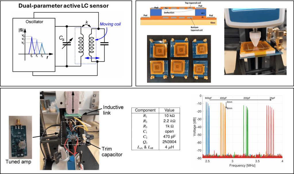
Wireless sensors have become essential components for a wide range of biomedical, agricultural, industrial and automotive applications. Typical wireless sensors face power and cost limitations due to the integration of sensing elements, readout electronics, conversion, and wireless transmission stages. In contrast, LC sensors combine a sensing capacitor and two mutually coupled inductors. One of the inductor coils is connected to the capacitor and forms a LC tank, while the other coil is used to readout the resonant frequency of the LC sensors. Changes in the target parameter are represented by a change in capacitance and translated to a shift in the resonant frequency of the LC sensor, making these sensors highly sensitive to specific parameters, including pressure, strain, humidity, temperature, gas, and touch. In addition to high-sensitivity, passive or semi-passive LC sensors, such as radio-frequency identification (RFID) tags, can be operated without a power source, whereby real-time parameter sensing is achieved via backscattering from an external reader. We are expanding the functionality of LC sensors to dual-parameter monitoring, where both L and C components can be adopted as sensors.
PROJECT: Dual-parameter LC sensor
Designers: N. Becker, S. Patel, Q. Currier-Moritsugu
Microscale inductive sensors have been recently proposed for pressure and displacement monitoring, creating opportunities for the development of novel LC sensors for a wide range of applications and monitoring conditions. Conventional inductive sensors consist of planar or 3-D coils, whose inductance varies with applied pressure or displacement. This type of sensor cannot be used in combination with capacitive sensors in LC circuits, since the resonance frequency will depend on both changes in inductance and capacitance. We have introduced an novel type of inductive sensor, consisting of an inductive link, with one moving and one fixed coil. Displacement of the moving coil results in changes of coupling are aligned in opposite directions to each other.
References:
● N. Becker, Q. Currier-Moritsugu and V. Valente. Tuned Amplifier With Embedded Dual-Parameter LC Sensor. IEEE Sensors Letters, vol. 9, no. 1, pp. 1-4, Jan. 2025, Art no. 5500304, doi: 10.1109/LSENS.2024.3508272.
● S. Patel, S. Darbasi, M. A. Antoniades and V. Valente. Inductively-Coupled MEMS Pressure Sensor. 2023 IEEE Biomedical Circuits and Systems Conference (BioCAS), Toronto, ON, Canada, 2023, pp. 1-5, doi: 10.1109/BioCAS58349.2023.10389171.
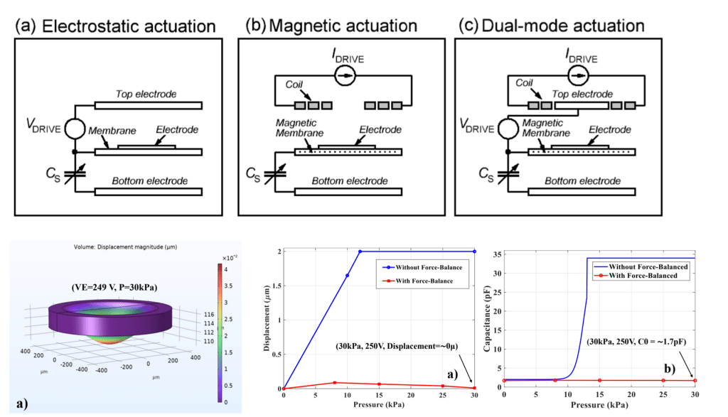
PROJECT: Force balanced LC sensors
Designer: S. Darbasi
Pressure sensors are universally adopted in a wide range of applications in the medical, industrial, agricultural, and commercial domains. Capacitive pressure sensors offer several advantages over other types of pressure sensors, such as piezoresistive, optical fiber, resonant, and piezoelectric sensors, including higher sensitivity, reduced temperature dependence, and lower power consumption. To achieve high sensitivity, pressure sensors need to be designed with a high aspect ratio (sensor area/membrane thickness) and small gaps. A high aspect ratio however limits the sensor pressure range due to its restricted deflection range and increased stress, with a risk of membrane rupture at higher pressure. Additionally, smaller gaps and thinner membranes enhance sensitivity but make the sensor more susceptible to mechanical fatigue and non-linearity in response. In a force-balanced mechanism, the external force acting on a system is actively counteracted by a feedback generated force to maintain the system in a stable or near-zero deflection state. By keeping the sensing element stationary or within a controlled operating point, the system achieves higher accuracy, faster response, and greater long-term stability. We are exploring the combination of electrostatic and magnetic force-feedback configurations. Electrostatic actuators are well suited for high-sensitivity, low-pressure adjustments due to their fine force resolution, whereas electromagnetic actuators provide a faster response and are more effective for high-pressure compensation due to their higher force output. The proposed dual-actuator configuration enhances the dynamic range of the sensor while maintaining high sensitivity at low pressures, and improving both accuracy and robustness in demanding applications such as medical ventilation, microfluidics, and industrial pressure monitoring.
References:
● S. Darbasi, Y. S. Shama, E. Abdel-Rahman and V. Valente. Design and analysis of a dual-actuator force-balanced MEMS pressure sensor. 2025 J. Micromech. Microeng. 35 085001.
